


Products
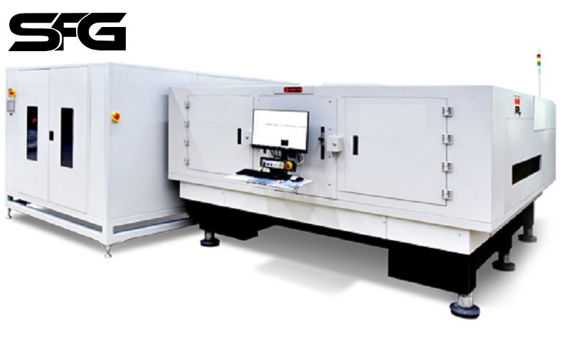
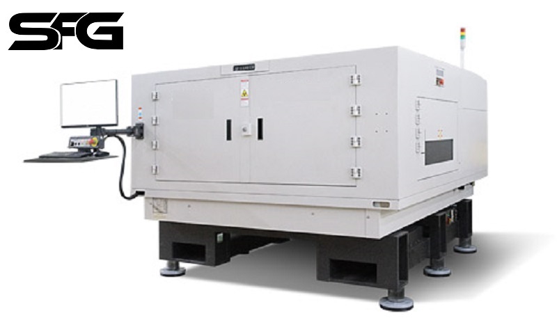
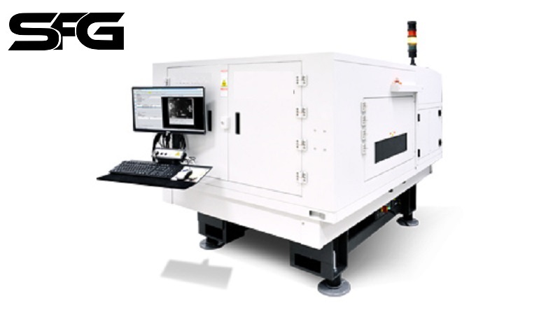
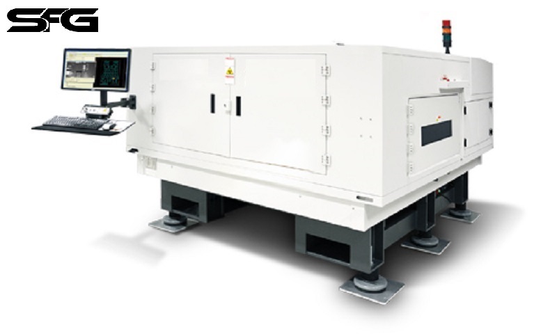
Advanced 3D X-ray Inspection System (AXI) S5810i S3 fast and good test coverage AXI system for SMT PCB assembly line
| System | S5810i S3 |
| System controller | Integrated controller with 8 Core Intel Xeon processors |
| Operating system | Windows 10 Pro (64 bit) |
| Test Development Environment | |
| User interface | Microsoft Windows based software solution with easy-to-use GUI and password-protected user levels |
| Off-line test development software | Optional for off-line PC |
| CAD conversion tool | Support 4 different types of CAD in V810i software and optional software available to translate other CAD data to ViTrox’s format |
| Typical test development time | 4 hours to 1.5 days to convert raw CAD file and develop application |
| Line Integration | |
| Transport heights | 865mm-1025mm |
| Line communication standard | SMEMA, HERMES |
| Barcode readers | Compatible with most industry standard barcode readers |
| Performance Parameters * | |
| False Call rate | 500-1000ppm |
| Minimum features detection capability | |
| Joint pitch1 | 0.3mm and above |
| Short width2 | 0.045mm |
| Solder thickness | 0.0127mm |
| Allowable Panel Characteristics ** | S5810i S3 |
| Maximum PCB Size (L x W) | 725mmx482.6mm (28.5″x19″) |
| Minimum PCB Size (L x W) | 63.5mmx63.5mm (2.5″x 2.5″) |
| Maximum PCB inspectable area | 725mmx474.9mm (28.5″x18.7″) |
| Maximum PCB thickness | 7mm (276 mils) |
| Minimum PCB thickness | 0.5mm (20 mils) |
| PCB warp | Downside < 3.3mm; Upside < 3.3mm |
| Maximum PCB weight | 4.5kg |
| Top Clearance of PCB | 50mm @ 22μm resolution |
| 42mm @ 19μm resolution | |
| 26mm @ 15μm resolution | |
| 11mm @ 12μm resolution | |
| 26mm @ 10μm resolution | |
| 11mm @ 7μm resolution | |
| (calculated from board top surface) | |
| Bottom Clearance of PCB | 80mm |
| PCB edge clearance | 3mm |
| 100% Press-fit testability | Yes (With PSP2 / PSP2.1 feature) |
| PCB Temperature | 40℃ |
| Installation Specification | |
| Power Supplies | 200–240 VAC three phase; 380–415 VAC three phase wye (+/- 5) (50Hz or 60Hz) |
| Air requirement | 552kPA (80psi) compressed air |
| System footprint (Width X Depth X Height) | 1835mmx2185mmx2162mm |
| Total system weight | ~4800kgs |
| **Note: | |
| 1. Panels are handled on width edges. Panels with edge cut outs may require the use of a carrier. | |
| 2. Maximum panel size dimensions and weight must include carrier if applicable. | |
| 3. Smaller panels are possible with the use of panel carriers. | |
| 4. With panels of this thickness, imaging results can be affected by PCBA layout. | |
| 5. Measured from the bottom of the panel including a maximum warp. | |
| *Note: | |
| 1. Assuming pad width is 50% of pitch. | |
| 2. The reported values for minimum feature detection assume that the feature is in a single plane of focus and that there are no X-ray absorbers in the X-ray path or in the immediate area of the feature other than those found in a typical multi-layer printed circuit board. | |
| #2×2 binning camera configuration. Hardware upgrade is required on old system. | |
Write your message here and send it to us